Expo Graphite and Composites
Leading the Way in Cutting-Edge Semiconductors
Welcome to Expo Graphite and Composites,our trusted partner in revolutionizing the semiconductor industry. We specialize in advanced materials and innovative solutions that drive the development of high-performance, reliable, and efficient semiconductor technologies. From silicon wafer manufacturing to epitaxial growth, our expertise and cutting-edge products set the standard for excellence in this dynamic field.
Request QuoteWhat is the Semiconductor Industry?
The semiconductor industry is a cornerstone of modern technology, responsible for designing, developing, and manufacturing semiconductor devices—tiny, highly specialized components that conduct electricity under specific conditions. These devices, including transistors, diodes, and integrated circuits, form the foundation of virtually all electronic systems. From powering smartphones, laptops, and gaming consoles to enabling advanced applications in automotive systems, medical devices, and renewable energy infrastructure, semiconductors are critical to global innovation. The industry encompasses material sourcing, wafer fabrication, chip design, and packaging, with a focus on improving performance, reducing size, and increasing energy efficiency to meet the demands of a rapidly evolving technological landscape.
What is the Silicon Semiconductor Manufacturing Process?
Polysilicon Manufacturing
Raw silicon from sand is chemically purified via the Siemens process to produce ultra-pure polysilicon, the base material for semiconductor-grade wafers.
Silicon Crystal Growth
Polysilicon is melted and shaped into a single-crystal ingot using the Czochralski process, forming the foundation for high-performance semiconductor wafers.
Deposition or Epitaxy on Wafer
Sliced wafers are layered with materials like silicon dioxide using deposition or epitaxy, building essential structures and enhancing electrical characteristics.
Photolithography
A photoresist-coated wafer is exposed to UV light through a mask, defining intricate nanoscale circuit patterns on the wafer surface.
Precision Etching
Etching removes selected material using wet chemicals or plasma, forming the tiny pathways that define transistors and circuit features.
Ion Implantation
Charged ions are embedded into specific regions of the wafer to adjust conductivity, enabling creation of p-type and n-type semiconductor areas.
Annealing Techniques
The wafer is heat-treated to activate implanted ions and heal crystal damage, ensuring proper electrical function and structural integrity.
Wafer Dicing and Packaging
Completed wafers are tested, cut into chips, bonded to connectors, and packaged for protection, ready for use in electronic devices.
How to Enhance Semiconductors and Silicon Wafer Manufacturing?
Improving Quality and Efficiency in Silicon Wafer Manufacturing
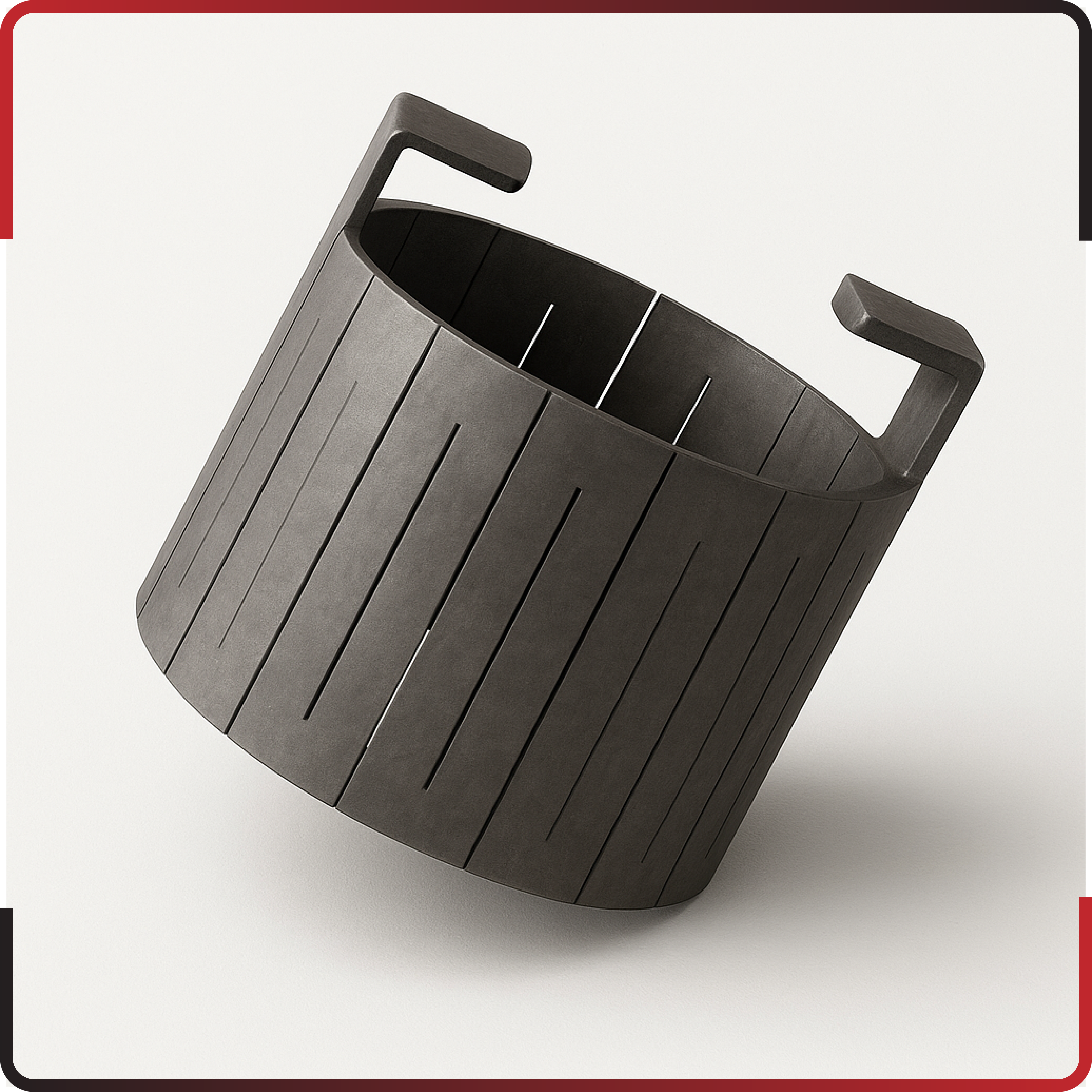
- High Temp Purification of Graphite: Graphite, a key material in semiconductor manufacturing, must be free of impurities to prevent contamination. High-temperature purification, often exceeding 2,500°C in a vacuum or inert gas environment, removes volatile contaminants and trace metals from graphite. This results in ultra-pure graphite components that enhance the reliability and yield of silicon wafer production, ensuring consistent quality for downstream processes.
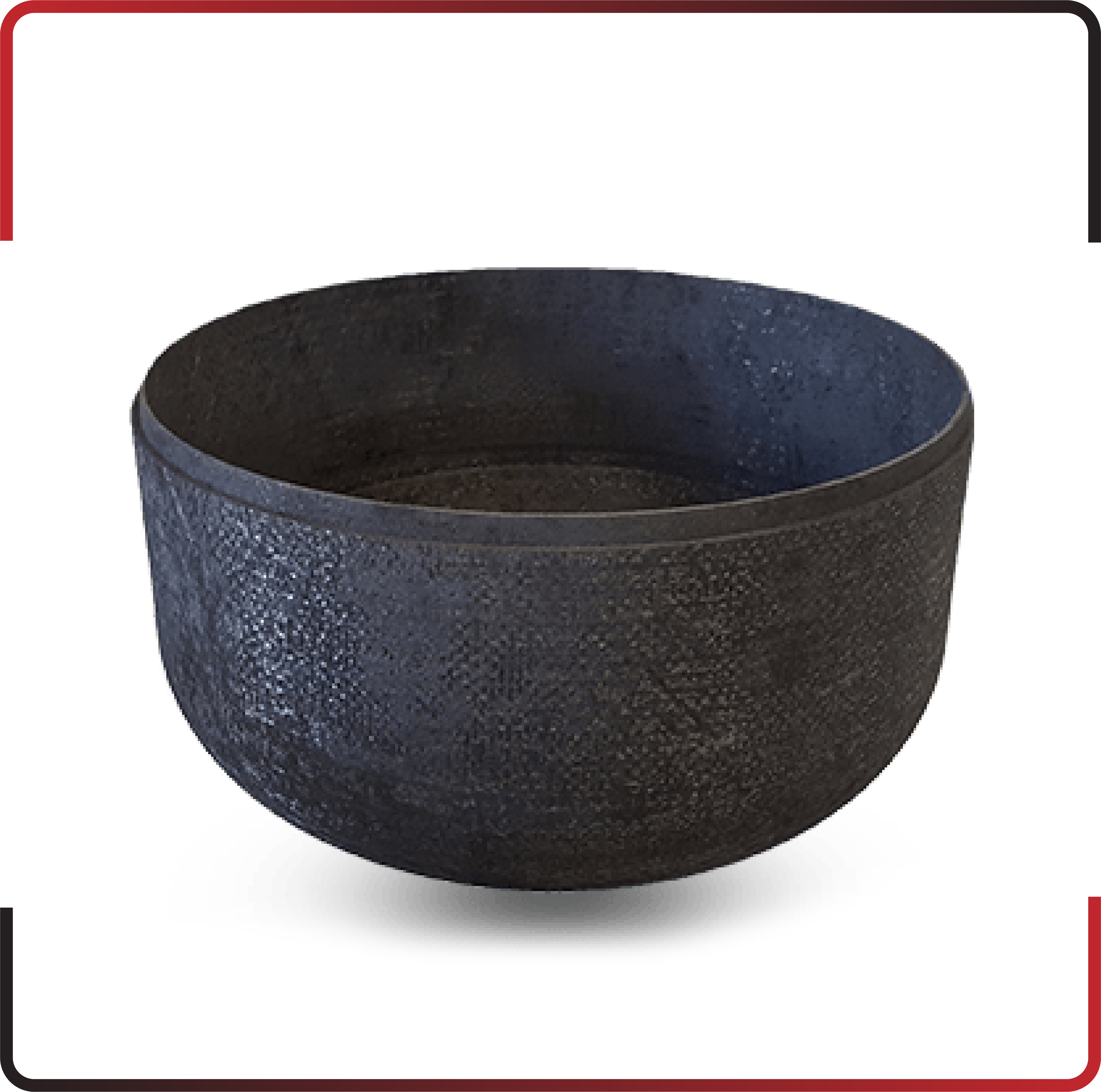
- Protecting Graphite with SiC Coating and TaC Coating:Graphite components, such as crucibles and heaters, face extreme temperatures and reactive environments. Coating them with silicon carbide (SiC) or tantalum carbide (TaC) provides a protective barrier. SiC coatings resist oxidation and chemical corrosion, maintaining structural integrity in harsh conditions. TaC coatings offer exceptional thermal stability and durability, withstanding temperatures above 3,000°C, extending the lifespan of graphite tools and maintaining process consistency.
- Elevating Silicon Crystal Properties Through Epitaxy: Epitaxy involves growing a thin, crystalline layer of silicon or other materials on the wafer surface. Advanced epitaxial techniques, such as molecular beam epitaxy (MBE) or metal-organic chemical vapor deposition (MOCVD), precisely control layer thickness, composition, and doping. This enhances the electrical, thermal, and structural properties of silicon, enabling faster, more efficient chips for applications like microprocessors and memory devices.
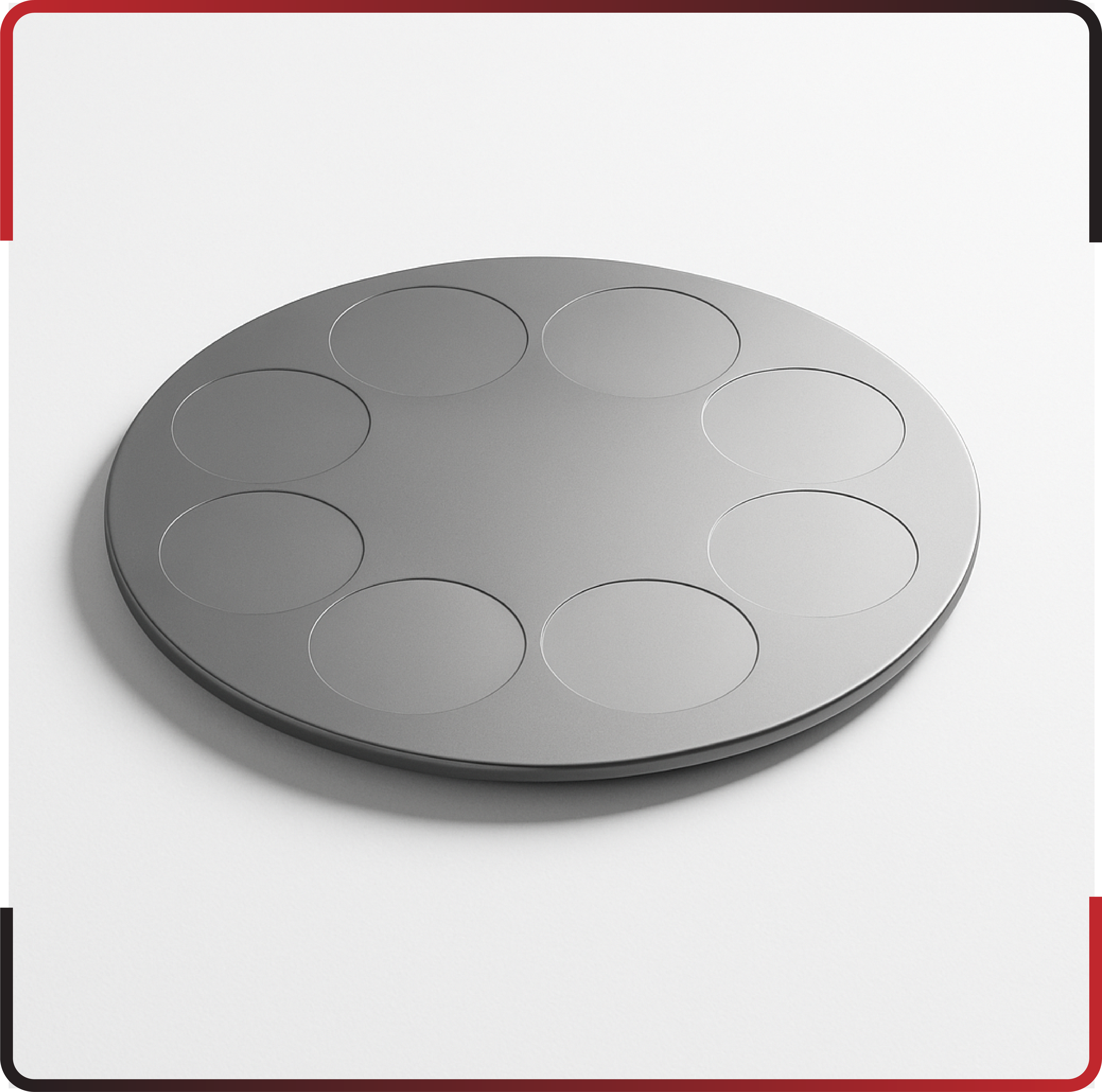
- Enhancing ALD Processes with Graphite Susceptor: Atomic layer deposition (ALD) is a precise technique for depositing ultra-thin, uniform layers of material. Graphite susceptors—specialized platforms that hold wafers during processing—provide excellent thermal conductivity and stability. Our high-quality graphite susceptors ensure even heat distribution, improving ALD uniformity and enabling the production of advanced, nanoscale semiconductor features critical for modern chips.
- Advancing SiC Epitaxial Layering for Enhanced Performance: Silicon carbide (SiC) epitaxy involves growing crystalline SiC layers on wafers, ideal for high-power, high-frequency, and high-temperature applications. By optimizing growth conditions—such as temperature, pressure, and gas composition—we enhance the quality of SiC layers, reducing defects and improving electrical performance. This drives innovation in power electronics, 5G components, and electric vehicle systems.